
A long time ago I heard a nice story about a fab manager in a company that I worked for.
This manager had a reputation of often (seemingly?) falling asleep during the weekly manufacturing meeting. One day, while he had dozed off, the yield team presented the usual numbers of the week’s lowest, average and highest wafer yields, the latter of which being 102%. That was the very moment when the fab manager woke up, shouting: “What?? 102%? You’re [expletive] me !!!”
Wafer yield appears to be easy to calculate:
The biggest problem with determining this calculation is the denominator.
The number of good devices listed in the numerator are found in the tester results file and are defined as all devices that fulfil the specified test criteria. There can be issues with the wafer probing, bad contacts etc., that may trigger retests, but once the test results are established, we know how many good devices are found on a given wafer. Even if we need to screen out some marginal, potentially quality-compromised parts, this is a fairly deterministic mathematical process.
The total number of devices on the wafer is, somewhat surprisingly, more difficult to establish. The problem with determining this number lies on the edge of the wafer. There is usually a zone of a few millimeters on the edge of the wafer where chemicals are removed. Devices that are printed partly in this area are not expected to work. Sometimes even devices that are fully printed but are close to this “edge exclusion zone” are also not expected to work. Hence, devices on a x/y-location on the wafer edge that never pass the testing process are sometimes subtracted from the total number of devices. This is what had happened in the story above – devices on locations that had never passed a test before, that were therefore not included in the denominator, had surprisingly now passed the test sequence, hence the wafer was yielding more than 100%.
The problem with the denominator becomes even more complex if we consider the fail rates of individual tests in the test sequence. This fail rate reflects the fact that in most production tests the test sequence is stopped after the “first fail”.
Consider testing a wafer with a total number of 1,000 devices. Now, when the first test is executed, we may have 200 failing devices. These devices will usually not be checked with further tests in the sequence. Let’s say of the remaining 800 devices, 80 fail the second test. What do we report as the fail rate of the second test?
Possible answers to this question are:
- The fail rate is 8%, as 80 out of a total of 1,000 devices failed the second test.
- The fail rate is 10%, as 80 out of 800 tested devices failed the second test.
The problem aggregates further when we continue in the test sequence. Interestingly, there seem to be no standards for calculating the fair rate in the industry. As a result, we go over these questions with each new customer, as we need to set the proper reporting options in YieldWatchDog to match the customers’ practices.
There is, however, one way to report the whole test sequence that doesn’t need any configuration, because it captures the whole picture:
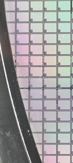
A close look at devices on the edge of 200mm wafer. Not all devices that appear to be fully printed are expected to work if they are too close to the edge.
It is one of my favorite tools in YieldWatchDog. It’s called “Cascaded Passes”, but is more commonly known as a “Waterfall Chart”:
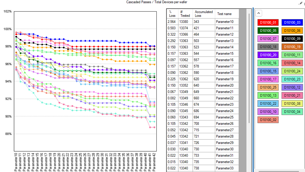
In this chart, you can see the test sequence plotted on the x-axis. The remaining passing devices are plotted in separate colors for each wafer on the y-axis. Using this chart, we can immediately discern high- and low yielding wafers and tests that cause significant yield loss on each of the wafers. The table also shows absolute and relative yield loss, so we have all the information we need to prioritize working on yield improvement.
Please note that we have left room on the yield axis for wafers that reach 102%. 😉