
Spatial Signature Control
Spatial Signature Control
Detect, mark, edit, and search for recurring spatial patterns — radial, edge, and repeating signatures — across every wafer in your database, with email alerts the moment a pattern matches. Optionally extends into AI-driven classification and clustering of pattern data for deeper analysis.
Capabilities
Spatial Signature Control: what it does
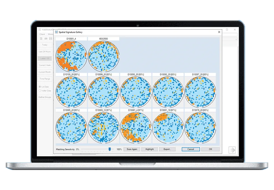
- Configurable signature detection — neighborhood window size, edge exclusion, fail-bin threshold
- Similar patterns are found automatically — no teaching needed, independent of product layout, shot map and angular orientation
- Matching runs each time a lot is imported; known patterns are kept in a pattern library
- Adjustable matching sensitivity to search for the same pattern across every wafer
- Manual signature editing to refine or correct auto-detected patterns
- CS (Characteristic Signature) parameter tracks a known pattern’s recurrence and severity over time, directly in the Trends View
- Email alerts the moment a pattern matches
- Optional AI-driven classification (rule-based and data-driven) for rapid material review and wafer disposition
- Material Review finds known and previously unknown patterns for hard bins, soft bins and parameters
- Pattern monitoring can also be applied to the spatial distribution of parametric values, for the earliest possible detection
Related pages
Support
Direct support from our experts
A direct technical contact who understands the software and the industry — no ticketing queue, the same level of support regardless of company size.
See it working on your own data
Low-cost trial installations are available. Our team will write the loaders and parsers for your data during the installation.
Schedule DemoFAQ
Frequently asked questions
How does Spatial Signature Control find patterns on wafers?
Spatial Signature Control monitors and detects equipment-specific spatial signatures in wafer test data, long before they are visible on wafer bin maps. It supports three applications: identifying wafers with similar patterns on bin maps, monitoring bin maps for known patterns that are defined manually or identified automatically from a reference wafer, and monitoring the spatial distribution of parametric values of chip-level test data for the earliest possible detection. Detection is independent of the product layout and shot-map setup and works regardless of the angular orientation of the pattern. Matching runs each time a lot is imported into the database, and matching sensitivity and neighborhood window size are configurable.
Do I have to teach the patterns first?
Not for the search for similar patterns: similar patterns on bin maps are detected automatically, without teaching them first. For known signatures you can mark a pattern manually with a brush, or let the software identify the signature automatically from a reference wafer using a share of failing bins and a neighborhood window that you configure, then name and save it in the pattern library. The matching sensitivity can be adjusted so that you decide how strictly wafers must resemble a pattern. A CS (Characteristic Signature) parameter then tracks how strongly and how often a known pattern appears over time, directly in the Trends View.
What happens when a pattern matches?
When the software finds matching patterns, it sends an email notification. In the Spatial Signature Gallery you can review the matching wafers with their match percentage, highlight the pattern, scan again with a different sensitivity and export the matching lots and wafers as CSV. The Spatial Signature Review shows reference patterns together with all matching wafers, and Material Review finds known and previously unknown patterns for hard bins, soft bins and parameters. Optionally, AI-driven classification supports rapid material review and wafer disposition, so engineers can decide quickly which material to hold.