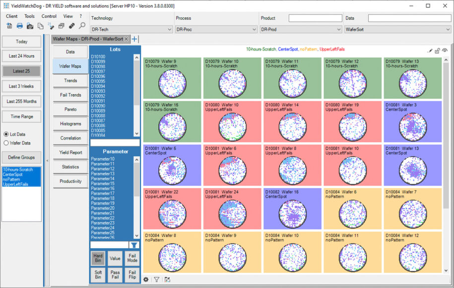
Searching through wafer maps looking for spatial patterns is not only a very time-consuming task to be done manually, it’s also prone to human oversight and error, and nearly impossible in a large fab where there are thousands of wafers a day being processed.
Our Spatial Wafer Pattern Detection & Classification tool is a classic Machine Learning/neural network application.
We developed a tool that applies automatic spatial pattern detection algorithms using ML, parametrizing pattern recognition and classification algorithms to work in a semiconductor manufacturing environment. Any user can deploy these algorithms within our YieldWatchDog software, right out of the tool.
In the video below, you see a small gallery of wafer maps. The user selects, for example, unsupervised clustering and in the background the ML algorithm fires off and clusters these wafers. Wafers with similar patterns are automatically found and classified by the tool, as you can see by the background colors behind the wafer maps. It’s as simple as that. You don’t need to be a data scientist to benefit from Machine Learning.
About DR YIELD software & solutions GmbH
DR YIELD provides the leading-edge advanced analytics software YieldWatchDog for analysis and control of semiconductor manufacturing and test data. This enables semiconductor manufacturers as well as Fabless companies to improve important manufacturing dimensions such as equipment availability, throughput, operating costs and yield. Once installed YieldWatchDog allows you to get actionable insights into your data. For detailed information click here.


