Early detection and analysis of process excursions decreases wafer scraps, prevents yield loss and saves engineering and manufacturing resources
Process excursion, or any deviation in a certain process, significantly impacts the cost of semiconductor manufacturing process and product yield.
During production, process excursion can be detected early during in-line inspections. However, in some cases, excursion isn’t detected until later in the production process such as during wafer testing in the probing area after production. Apart from that, a timely detection of process excursion requires substantial engineering resources.
With effective yield management and the implementation of systems to maintain yield and quality levels, excursions in semiconductor manufacturing are readily detected. The main systems used to prevent excursions are the statistical process control (SPC) and advanced process control (APC).
Excursion Prevention
Detecting and containing process excursions is facilitated using advanced statistical analysis of manufacturing process data and by applying statistical process control (SPC) and advanced process control (APC).
Statistical process control (SPC) is the most commonly used system in manufacturing.
Although SPC in manufacturing is mainly used for defect counts and in-line wafer measurements such as critical dimensions, modern systems allow the application of SPC for electrical wafer test data.
Apart from SPC, another system for maintaining yield and quality levels is the advanced process control (APC). APC includes tools such as fault detection and classification (FDC), virtual metrology (VM), and run-to-run (R2R) control.
To prevent process excursions, fault detection and classification (FDC) uses statistical methods to monitor equipment parameters such as temperature, pressure and other sensor data in the wafer processing. The goal of FDC is to eliminate undesired process conditions faster than with traditional methods.
Virtual metrology (VM) exploits sensor data from the equipment and calculates resulting wafer properties such as deposited thickness layers.
Run-to-run (R2R) control is the continuous adjustment of process parameters based on measurements of previously processed lots or wafers.
Preventing process excursion with a yield management software
Process excursion is visible in the process data. However, besides confirming the excursion, it is key to identifying which wafers have been affected.
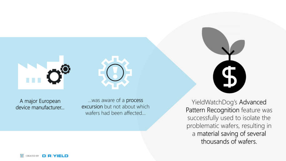
“We had a case where a major European device manufacturer was aware of a process excursion but not about which wafers had been affected. With advanced pattern recognition, the customer successfully isolated the problematic wafers which resulted in a material saving of several thousands of wafers.”, says Dieter Rathei, the CEO of DR YIELD.
The pattern recognition is an advanced AI tool in a yield management software that increases efficiency by detecting and classifying spatial patterns on the wafers. The pattern classification is automated which ensures process and yield engineers to save time while the software automatically classifies patterns in few seconds or minutes depending on the data size. Additionally, the automatic pattern classification groups all the wafers with the same pattern, which enables an advanced in-depth analysis and comparison.
Process excursions can impact product wafer sort yield as well as manufacturing costs. Thus, determining the root cause of process excursions allows engineers to create actionable plans to improve the semiconductor manufacturing process and prevent future process excursions.


